&width=180&quality=85&format=auto)
Transmission electron microscopy for materials science
The Non-degree in Transmission electron microscopy for materials science at École polytechnique fédérale de Lausanne (EPFL) is a 1 week long program for international students taught in English.
Introduction
About the Program
Similar Programs You Can Apply To
Direct application via Global Admissions is not available for this program. Browse similar partner programs below or visit the university's site to apply directly.
Thompson Rivers University
Bachelor in
Tuition
2,095 USD / year
University of Stirling, UK
Master in Disaster Interventions and Humanitarian Aid
Tuition
24,430 USD / year
University of Cologne
Master in "Ecology, Evolution, and Environment"
Emory University, Atlanta
"Making" Progress Teach-Out
Tuition
$120 USD
University of Cologne
Master in "Management, Economics and Social Sciences"
EU Business School
Bachelor in (Hons) in Business Management (Business Technology)
Tuition
6,964 USD / year
Related Blog Posts

30 Fun Facts about Switzerland
December 15, 2024

5 Japanese Universities Offering Application Fee Waivers for International Students 2026
May 10, 2026
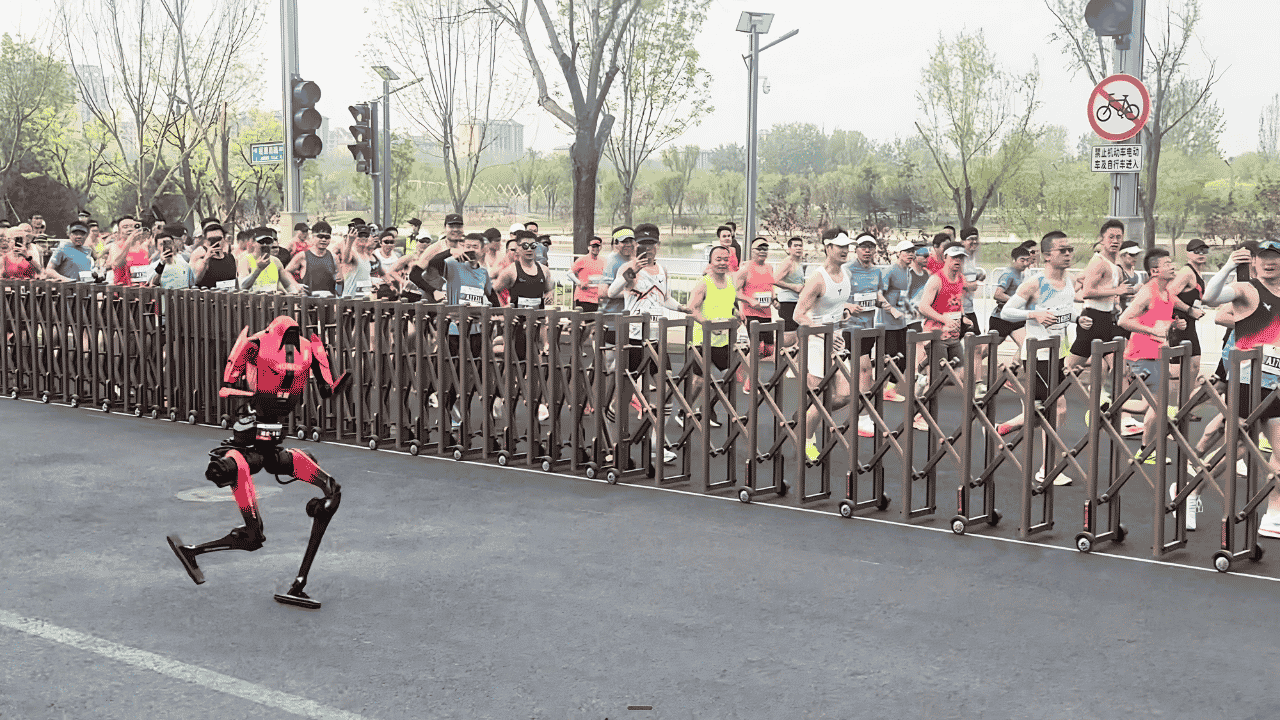
China Is Racing Ahead in AI and Robotics – And Drew a Line Around AI Replacing Workers
May 9, 2026

9 Underrated Destinations for International Students in 2026
May 2, 2026
-
Deadline
- Anytime
- Tuition
- $120 USD
-
Application Fee
- 0 USD
-
Service Fee
- 0 USD
Why Apply on Global Admissions?
- Boost Your Acceptance Rate
- Easy Online Application
- Thousands of international students use Global Admissions with 4.9 star reviews
- Free Service to Partner Universities or upgrade to our Premium Admissions Service